High Performance
On-Chip Memory
Supports FIXED, INCR, and WRAP bursts
Simultaneous Read/Write
Optimize for throughput
For program execution, data storage
Memory-mapped addresses
FULL DATASHEET
AXI4 Memory Controller IP Core
ASIC and SoC designs require on-chip memory for on-chip program and data storage to gain high-performance and low power advantages. To reduce risks, chip designs are usually emulated in FPGA hardware for thorough testing before taping out. Thus, on-chip memories use FPGA-like RAMs which are later replaced with silicon process' RAMs. LeWiz's AXI4 Memory Controller IP core enables the customer to emulate in FPGA and move ASIC designs to the silicon process seamlessly -- 1 code flow from simulation, emulation to ASIC tape out; reducing risk of human errors.
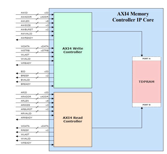
Advanced eXtensible Interface 4 (AXI4) is widely used with on-chip modules. It allows for ease of integration, greater bandwidth with large data transfers (bursts) and parallel read/write accesses - supporting true dual-port RAM (TDPRAM). LeWiz IP core uses AXI4 bus for interfacing to customer's internal bus. It can be used with RAMs generated from the RAM compilers which may be available from the foundries or other providers.
Applications for LeWiz AXI4 Memory Controller range from microcontroller designs, to DSP chips, to integrated SoCs for high performance systems and others. The design of the AXI4 Memory Controller is tuned for low latency, simultaneous reads/writes, efficient bus cycle, burst accesses, and fast data transmission through bidirectional data transfers. It supports memory-mapped addressing -- simple and efficient decoding.
- FEATURES:
- Well known AXI4 protocol interface
- Simultaneous read/write accesses
- Supports burst data transmissions
- FIXED, INCR, WRAP burst modes
- Supports narrow-lane, unaligned, unaligned narrow-burst transfers
- Optimize for high performance, low power
- Can specify ID, Address, Data Bus width + TDPRAM depth
- Automatic AXI4 controller data width matches TDPRAM
- Automatic corresponding AWSIZE/ARSIZE value to bus width
See datasheet for more information.