- High speed and low power consumption
- 12 nm FinFet Technology
- High bit rate
- High noise immunity
- Differential signal pair on the external side to interface to external component
- Single-ended on the internal side interfacing to user's internal logic
FULL DATASHEET
LVDS Transceiver IP Core
High speed transceiver circuits are analog. Their designs require specialized knowledge and transistor-level tuning for specific silicon process. This product is available in Global Foundries 12LP process and others.
High speed transceivers have many applications such as Ethernet networking, communication channel interfaces, bus interfaces, and others. They are also used for inter-chip connectivity from an A/D converter to a FPGA/processing chip or from an Ethernet MAC to PHY devices. They reduce the number of signals required for connecting from 1 chiplet to another in multi-chip modules. Many devices use high-speed transceivers including USB devices such as memory stick. Additional electronics such as HD displays, infotainment systems and industrial cameras use LVDS for its giga bit per second serial transmission. Other applications for LVDS include laptops, computers, networking, imaging, medical, and automotive.
Low-voltage differential signaling (LVDS) circuits are a class of high-speed transceivers enabling high bit rate (up to 10's of Giga bit per second), reliable data transfer through serial communication links. LVDS transceivers facilitate low power and point-to-point transmissions over long distance. Used in combination with fiber optic they can drive distances in the Kilometer(s) range. LeWiz is offering this as an IP core product to reduce customer complexity, debugging time and quicken time to market.
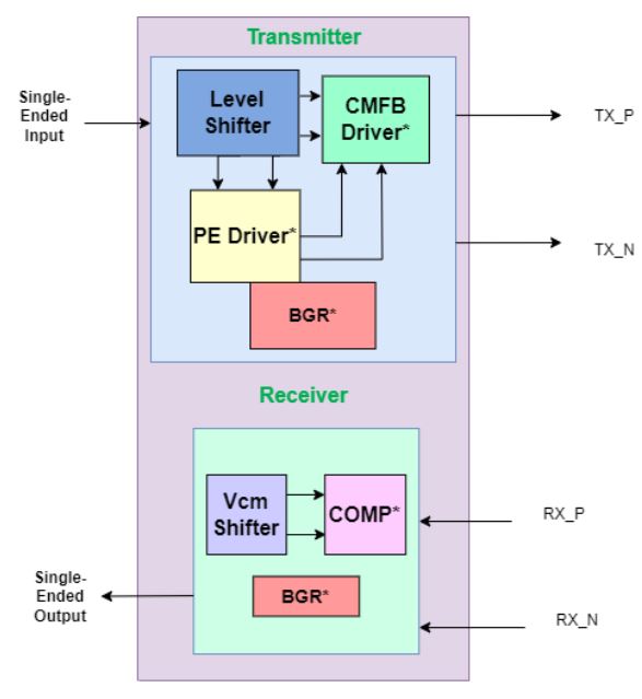
On the transmit side, LeWiz LVDS IP core translates the single-ended internal digital signal to differential with pre-emphasis capabilities and buffering to drive the high load line. On the receive side, the LVDS IP core receives the differential signal with equalization and converts the signal to be compatible with the silicon's internal voltage.
The IP core can be used in single or multi-lane configuration with commercial EDA tools from major vendors. Each lane supports up to 12.5Gbps rate (higher rate available based on customer requirements).
- 12.5 Gbps PMOS-based low-voltage differential signaling (LVDS)
- 12 nm FinFET technology
- Compatible with ANSI/TIA/EIA-644-A standard
- Compatible with commercial devices such as high-speed FPGA, ADC, DAC devices
- Support major commercial EDA tools
- provides a low-power and point-to-point transmission
- low power consumption
- low radiated EMI
- good noise immunity
- differential amplifiers, 100 Ohm differential line
- robustness to common-mode noise
- ESD protection circuit to the IC pins
- biasing circuit and amplification structure.
Features
See datasheet for more information.